Samsung Will Reportedly Use TSMC's 3nm Process for the Base Die in Nvidia's Custom HBM, Called NVHBM
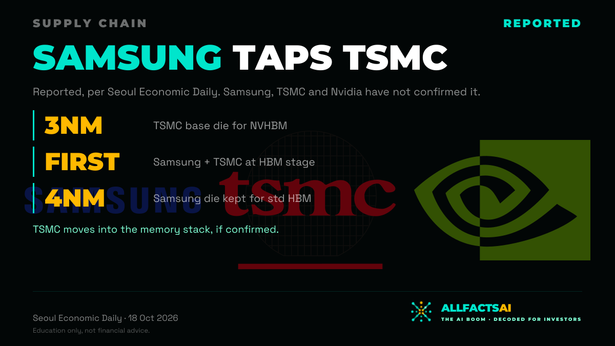
Reported, per Seoul Economic Daily (18 Oct 2026), and carried by Reuters: Samsung will use TSMC's 3nm process to make the base die for Nvidia's custom HBM, called NVHBM. It would be the first time Samsung and TSMC partner at the HBM manufacturing stage. Nvidia reportedly asked Samsung, SK hynix and Micron to use TSMC 3nm base dies and to standardise the core die on the 1c (sixth-gen) DRAM process. NVHBM is based on the HBM4E architecture. Nvidia unveiled NVHBM on 26 Aug 2026, which puts Nvidia's custom memory controller in the HBM base die. Samsung keeps its own 4nm foundry base die for standard HBM and for other customers, including AMD, and is checking whether its own foundry could also make NVHBM base dies. Samsung, TSMC and Nvidia have not confirmed the report.